
301 Moved Permanently
The current process for making solar modules involves four key steps: polysilicon production, ingot shaping and wafering, cell production and module production. This article will focus specifically on the wafering step, which can be accomplished via one of two methods.
To start, polysilicon is produced for use in the PV industry in ingots (solid rectangular or cylindrical silicon bricks). There are three key methods for making these ingots, and each produces silicon with different qualities. Monosilicon is the most uniform of the three; it is more expensive to make but results in higher efficiency cells. Multisilicon is less uniform, less expensive and less efficient. A newer type, called mono-like, combines properties of both the monosilicon and multisilicon processes, but it is not yet widely used.
The wafering process involves slicing the polysilicon ingot into thin wafers. The slicing is done by running a thin steel wire (SW) coated with a silicon carbide and oil slurry through the ingot. Slicing the ingots with diamond wire (DW) is a very similar process, but, in this case, a diamond abrasive is fixed to the wire - generally via an electroplating process.
DW has been widely discussed for a number of years as a possible replacement for SW and slurry for slicing silicon ingots into wafers. However, little evolution has occurred yet. In September 2012, I visited the 2012 EU PVSEC Conference to find out why this delay is occurring, whether the market will switch to DW, and when and to what extent this change will occur.
Virtually all wafers are currently sliced using the SW process. This process has remained relatively unchanged for over a decade, and the opportunity for cost reduction or productivity gains appear to be limited. As the scale of the industry has grown and as pressure on costs has mounted over the last three to five years, the industry has begun to look at alternative slicing tools.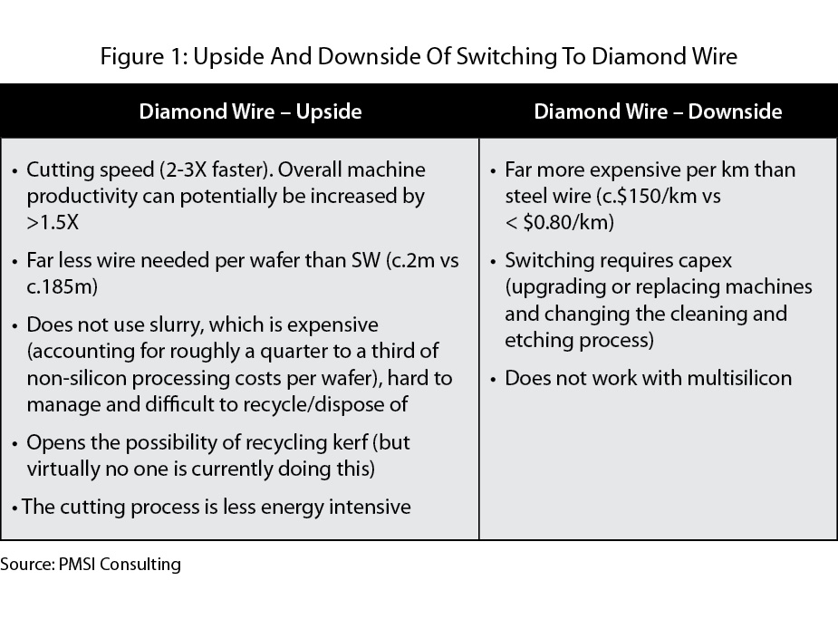
Fixed-abrasive DW offers three key benefits versus SW: It cuts two to three times faster, increasing machine productivity by more than 1.5 times; it does not use slurry, which is both expensive and difficult to manage; and far less material of it is needed per wafer. (See Figure 1.)
Lack of economics
The findings in this article are based on conversations with more than 50 market participants, including many of the world’s largest wafer manufacturers, machine manufacturers, SW and DW manufacturers, and industry experts and analysts. These discussions indicate that virtually all scale wafer manufacturers are testing DW in some capacity, but outside of Japan, almost no one is running it commercially. Why not?
There are two key reasons. First, the economics of DW have not stacked up until recently. While DW is more durable, offers productivity gains and removes the need for slurry, it is far more expensive per kilometer (km). This difference was significantly more pronounced 12 to 18 months ago, when DW cost more than $250-$300/km, versus approximately $1.28/km for SW.
Today, the cost difference has narrowed somewhat. Because DW accounts for a much higher proportion of the non-silicon processing cost (greater than 80%) than SW (30%), the drop in the price of DW has had a far larger impact on overall cost than it has for SW.
Although it is hard to make sweeping statements about the effect that this change will have on individual production lines, our general view is that switching to DW today can offer an approximate $0.10 in savings per wafer versus SW (assuming the production line is running wafer slicing machines specifically designed for DW). 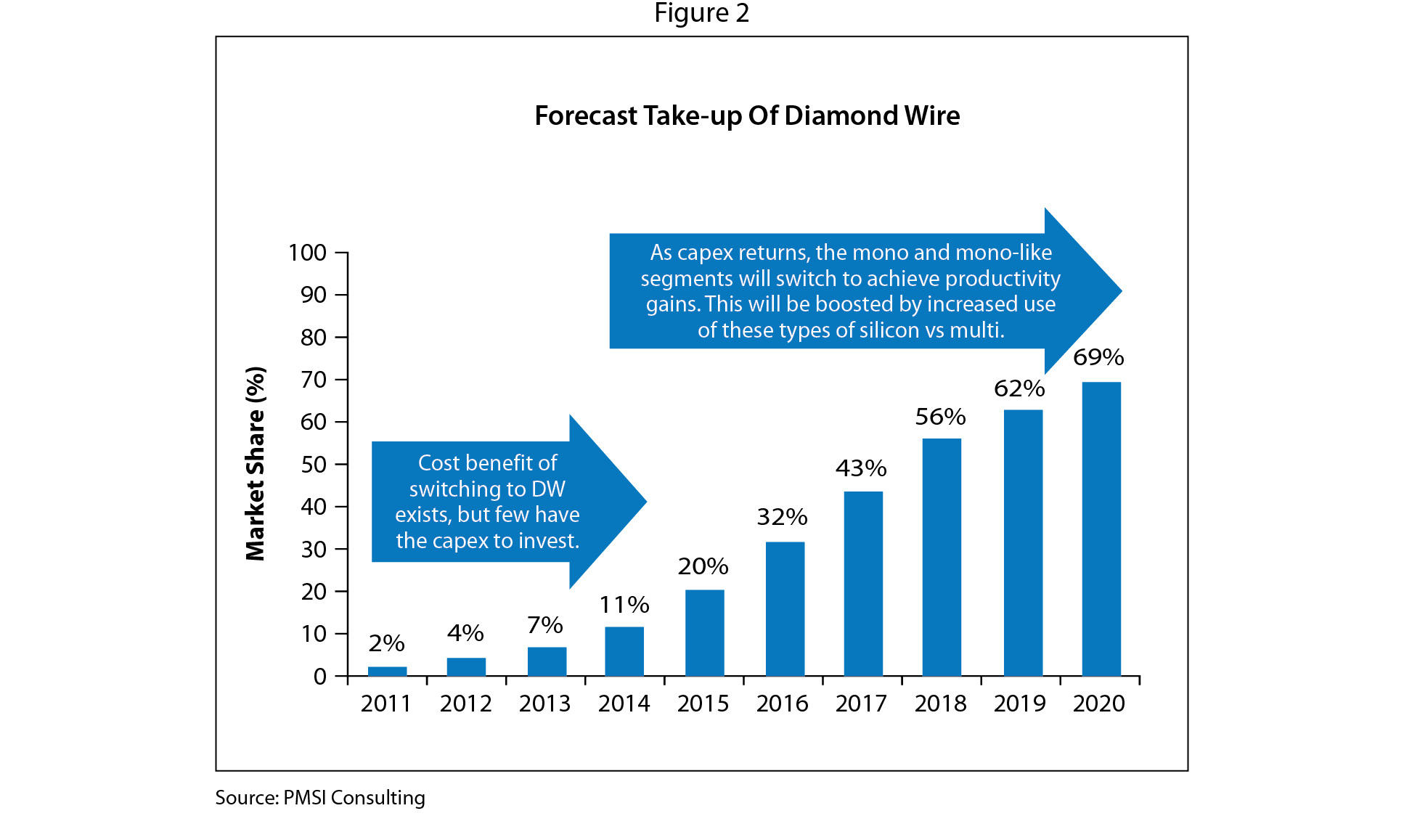
This can be a large absolute figure. For JA Solar, for example, which produces roughly 2.4 GW of wafers annually, the potential annual benefit of switching could be as much as $65 million per year. However, as we will discuss later, the reality for the time being is that JA Solar will only switch its mono and mono-like capacity.
In addition, the market currently lacks both the appetite and capacity to invest the required capex. Switching to DW will require significant refurbishment or, in most cases, replacement of wafer slicing machines. At close to $1 million per machine, this is a large outlay. It will also require changing the cleaning and etching process, which will be a cash outlay for cell manufacturers, who tend to be different companies.
The commercial reality is, even if the cash did exist in the market, any switch that required a capex program of this magnitude would face some stickiness as manufacturers looked to prove the process and product.
Supply side risk?
The other key factor that will limit the switch to DW is that, to date, it has not proven to be an effective cutting tool for multisilicon ingots. It results in a level of breakage, both in the wafering process and further down the production line, that more than offsets any productivity or cost benefit.
However, DW has been shown to work effectively with monosilicon - the Japanese market is proof of this - and is widely expected to work with mono-like. As a result, we group both types of silicon together in Figure 3.
This makes the type of silicon used in the market an important driver in the uptake of DW, but predicting which the market will favor in the future is a rough science at best. We adopt the view that the market will move in the direction of mono and mono-like wafers, which we estimate will account for approximately 60% of the market by 2017 or 2018 - up from 40% today. 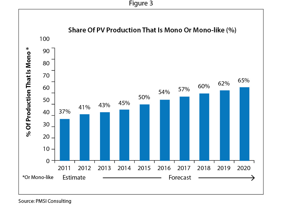
The other common issue raised by some wafer manufacturers was whether suppliers of DW would be able to meet demand if the industry did switch. Broadly speaking, we do not see this as an issue. Although Asahi appears to be the only player currently supplying commercial quantities of consistently high-quality wire (we estimate its market share is greater than 60%), rumor is it has plenty of spare capacity.
Moreover, there are other Japanese players making quality product that could expand capacity, including JFS, Noritake, Read and A.L.M.T. By 2014, the market will be far more competitive. Switzerland-based Meyer Burger has a clear and aggressive DW road map and, despite some concerns about the quality of its product, it is likely to be a major participant in this market.
Other European players, including Bekaert, Saint Gobain, Schmid and Log-o-Matic, are also likely entrants, alongside a cohort of Chinese and Taiwanese players, including DIAT and MDWEC.
Adoption of DW should begin in earnest around 2014, as capex returns to the market. By 2020, we forecast that 69% of wafers will be sliced using DW, using 25-34 million km of DW annually.
As mentioned earlier, the DW market is relatively nascent today. Our estimate is that it accounts for less than 5% of the market. We do not expect any dramatic change to this until 2014, when capex budgets should return as the current market turmoil eases. The market should then switch rapidly. 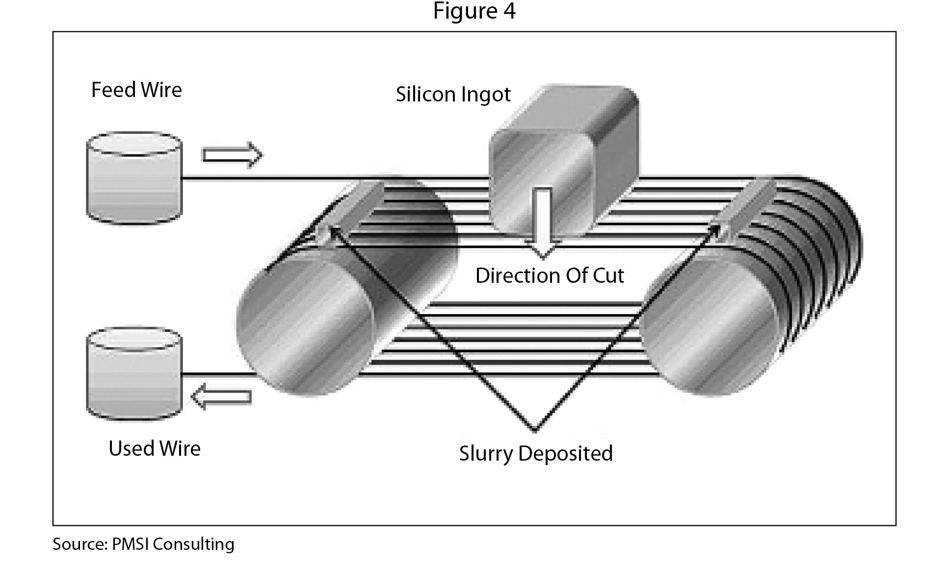
Our forecast is that DW will account for 11% of the market in 2014, 43% in 2017 and, finally, 69% by 2020. Most of this switch will happen in the mono and mono-like markets, which, by 2020, will almost solely be using DW. By contrast, we estimate DW will account for less than 30% of the multi market.
In overall volume terms, this will result in a very significant expansion in the volume of DW used, driven both by it replacing SW and by underlying growth in PV demand. It is estimated that the global solar PV market used around 0.3 million km of DW in 2011 (mostly in Japan) and 0.6 million km in 2012, and that it will use 2.7 million in 2014, 11 million to 14 million in 2017 and 25 million to 34 million by 2020. R
Process: Wafering
Manufacturers Will Slowly Switch To Diamond Wire
By Jacob Tyler
Why are many leading solar manufacturers still using slurry-based wafering processes rather than diamond wire?
si body si body i si body bi si body b
si depbio
- si bullets
si sh
si subhead
pullquote
si first graph
si sh no rule
si last graph