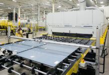
Arcadis, a global design and consultancy organization, will be providing full architectural and engineering design services to solar manufacturer CubicPV for its 10 GW silicon wafer manufacturing facility in the United States.
In addition to providing multi-disciplinary engineering, architecture, advanced industrial process design and project management services for the solar manufacturing facility, Arcadis will also engage with key stakeholders of the project, including construction contractors, agencies having jurisdiction and the local community. Arcadis’ experience is playing a critical role in bridging the project scoping and extensive front end engineering design work completed to date and executing the final phase of the design effort.
The Inflation Reduction Act represents the largest U.S. investment in clean energy to date and works to decarbonize the economy and respond to climate change. This investment includes the catalyzing of U.S. solar manufacturing and other renewables to meet the demands of the energy transition. For its part, Arcadis has played a strategic role in connecting private manufacturing clients with public sector clients around their decarbonization initiatives.
“With the initial phases of our engineering and design work complete, we knew we needed a firm of Arcadis’ caliber to carry the work forward and make it U.S. ready,” says David Gustafson, president of Cubic Wafer. “Their familiarity in executing large global projects, industry leadership, solid record in design and consultancy and focus on sustainability were deciding factors during the selection process. It’s an exceptional fit.”
Image by StockSnap from Pixabay.


